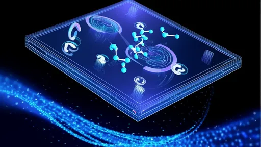
The field of quantum photonics has witnessed a remarkable convergence between two seemingly disparate domains: topological physics and integrated quantum optics. This synthesis has given birth to topological photonic chips - a revolutionary platform that promises to transform how we manipulate and control quantum light at the nanoscale.
At the heart of this innovation lies the elegant marriage of topological protection with quantum light sources. Traditional photonic circuits, while powerful, remain vulnerable to fabrication imperfections and environmental disturbances that scatter or dissipate precious photons. Topological photonic chips overcome these limitations by harnessing the robust propagation modes inherent in certain carefully engineered structures.
The quantum advantage of topological waveguides becomes particularly apparent when dealing with entangled photon pairs or squeezed light states. These fragile quantum states, essential for quantum communication and computation, can traverse sharp bends and defects in topological waveguides without backscattering or mode mixing. Recent experiments have demonstrated entanglement preservation over millimeter-scale propagation distances in silicon-based topological photonic circuits - a critical milestone for practical applications.
What makes these chips truly transformative is their scalability. Researchers have successfully integrated single-photon sources, topological waveguides, and detectors on a single chip using standard semiconductor fabrication techniques. This monolithic approach eliminates the losses associated with fiber coupling between discrete components and opens the door to complex quantum photonic processors with hundreds or thousands of components.
The materials landscape for topological photonic chips is rapidly expanding. While silicon-on-insulator platforms dominated early research, new material systems like lithium niobate, gallium arsenide, and even two-dimensional materials are showing promise. Each material offers unique advantages - nonlinear optical properties for photon pair generation, electro-optic tuning capabilities, or compatibility with specific quantum emitter systems like quantum dots or color centers.
One particularly exciting development involves the integration of quantum light sources directly into topological cavities. These hybrid systems combine the best of both worlds: the deterministic emission properties of quantum emitters with the exceptional quality factors of topological cavities. Recent theoretical work suggests that such systems could achieve near-unity beta factors - meaning virtually all emitted photons couple into the desired optical mode.
From a practical standpoint, topological photonic chips are solving some of quantum photonics' most persistent challenges. The notorious insertion loss problem in conventional photonic circuits, which often requires complex active stabilization, is mitigated by the intrinsic robustness of topological transport. Similarly, the phase stability requirements for quantum interference experiments are significantly relaxed when using topological components.
Quantum simulation applications are emerging as another promising direction. The mathematical equivalence between certain topological photonic structures and exotic quantum systems allows researchers to simulate complex quantum phenomena in a highly controlled environment. This includes the study of many-body physics, fractional quantum Hall effects, and even hypothetical particles like anyons - all on a chip-scale platform at room temperature.
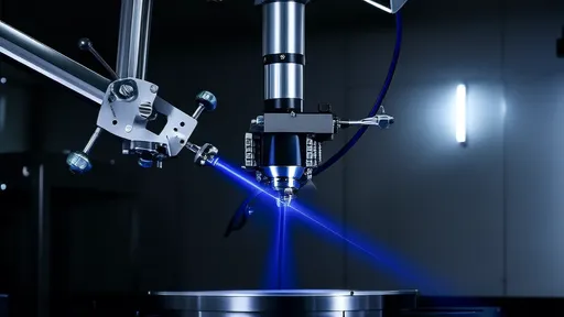
Manufacturing challenges remain, particularly regarding the precise positioning of quantum emitters relative to topological waveguides. However, novel techniques like in-situ electron beam lithography and pick-and-place assembly of pre-characterized quantum dots are showing encouraging results. The field is also benefiting from advances in inverse design algorithms that can automatically optimize topological photonic structures for specific quantum optical functions.
Looking ahead, the roadmap for topological photonic quantum circuits points toward increasingly complex functionality. Multi-layer integration, combining topological photonics with superconducting electronics for detection and control, and the development of topological nonlinear elements for all-optical quantum gates are all active areas of research. Some groups are even exploring hybrid quantum systems that interface topological photonic chips with atomic vapors or trapped ions for long-lived quantum memory.
The potential impact extends beyond fundamental research. Quantum communication networks could leverage topological photonic chips to create ultra-stable quantum links resistant to environmental perturbations. In quantum computing, these chips might serve as the optical interconnect between superconducting or trapped ion quantum processors. Even quantum sensing applications stand to benefit from the enhanced sensitivity and noise immunity offered by topological quantum photonic devices.
As the field matures, standardization efforts are beginning to emerge. Foundries are developing process design kits for topological photonic components, much like those available for conventional photonics. This will lower the barrier to entry and accelerate innovation, potentially leading to a new ecosystem of quantum photonic devices and applications.
The convergence of topology and quantum photonics represents more than just a technical advance - it's a fundamental shift in how we approach light manipulation at the quantum level. By providing a robust, scalable platform for quantum light control, topological photonic chips are poised to play a central role in the coming quantum technology revolution.

By /Aug 5, 2025

By /Aug 5, 2025

By /Aug 5, 2025

By /Aug 5, 2025

By /Aug 5, 2025

By /Aug 5, 2025

By /Aug 5, 2025

By /Aug 5, 2025

By /Aug 5, 2025

By /Aug 5, 2025

By /Aug 5, 2025

By /Aug 5, 2025

By /Aug 5, 2025

By /Aug 5, 2025

By /Aug 5, 2025

By /Aug 5, 2025

By /Aug 5, 2025

By /Aug 5, 2025
By /Aug 5, 2025
By /Aug 5, 2025